Designing and Construction of a Baby 8 Sequencer - Part II: Process
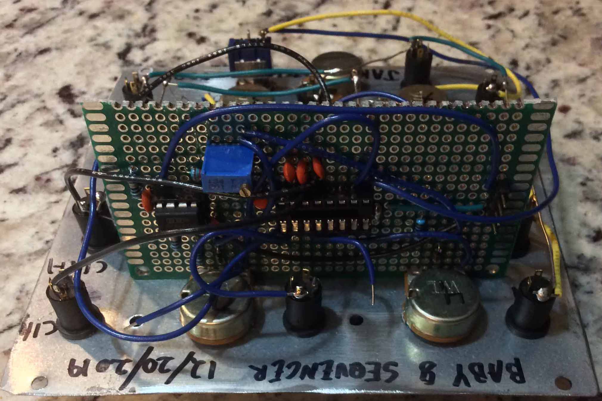
After spending substantial of time designing the Baby 8 Sequencer actually putting it together was an ambitious task. Unfortunately I designed the proto-board to attach perpendicularly to the potentiometers, and in a poor location. The bottom three rows of panel mount devices could, for the most part, be symmetrically jumpered together. This was easy, fun, and not overly time consuming due to the symmetry. The top row panel mount devices (sequence step 1 and 5) were above the proto-board so each connection had to be made directly to the CD4017 instead of to convient bus-bars. When I build a second sequencer, I will design a PCB so that each panel-mount device soldiers directly to the PCB. Replacing wires with PCB traces saves time.
Back of the Baby 8 Sequencer, a real rat’s nest.
The entire build process from cutting the panel, to debugging the circuitry took about 24 hours over the course of 11 days. A significant portion of time was spent pondering the optimal way to route the wires. Anyway, here’s my best advice if you want to do it yourself:
Label the function of each panel mount device on the backside of the panel. It's inevitable that you wire to the wrong device when you look at the mirror image of your design. I flipped the wiring for the 1st and 5th sequence step.
If you need to scale a DC voltage by a small amount (Less than 1 V), a super diode circuit doubles as a DC voltage shifter.
Just spend the few dollars and buy lots of different colored wires. It'll make debugging a lot easier.
Use resistors to eliminate floating points on digital control pins. The CD4017 IC has several control pins that I didn't need to interface with. Initially I did not wire them to anything. This creates floating points which are effectively random voltage levels. Random voltages create unpredictable circuit responses.
Each digital control input should have it’s own grounded 0.1 µF capacitor to smooth out signals.
Minimize incoming power cables by utilizing voltage regulators for IC’s.
Make as many processes as repeatable as possible. This goes for anything. If you can repeat something you can automate it. Repeatability makes error-checking easier, and manufacturing faster.
If your motivation for designing a module is to save money, find a new one. If it takes 24 hours to build a device yourself, you're far better working your day job for that amount of time and just buying a module. Even at minimum wage you’ll probably be ahead a few bucks.
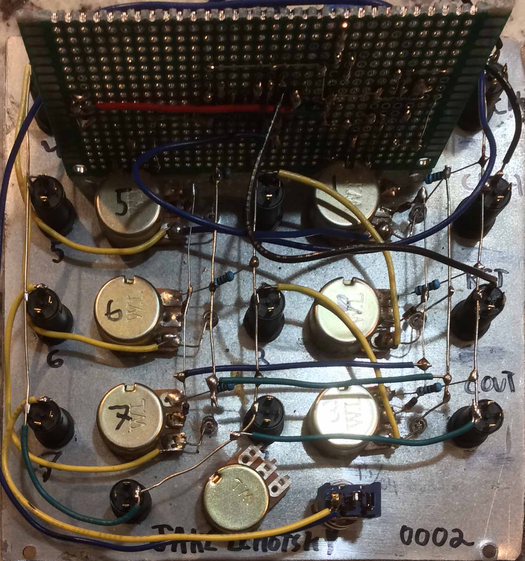
Nice neat circuit
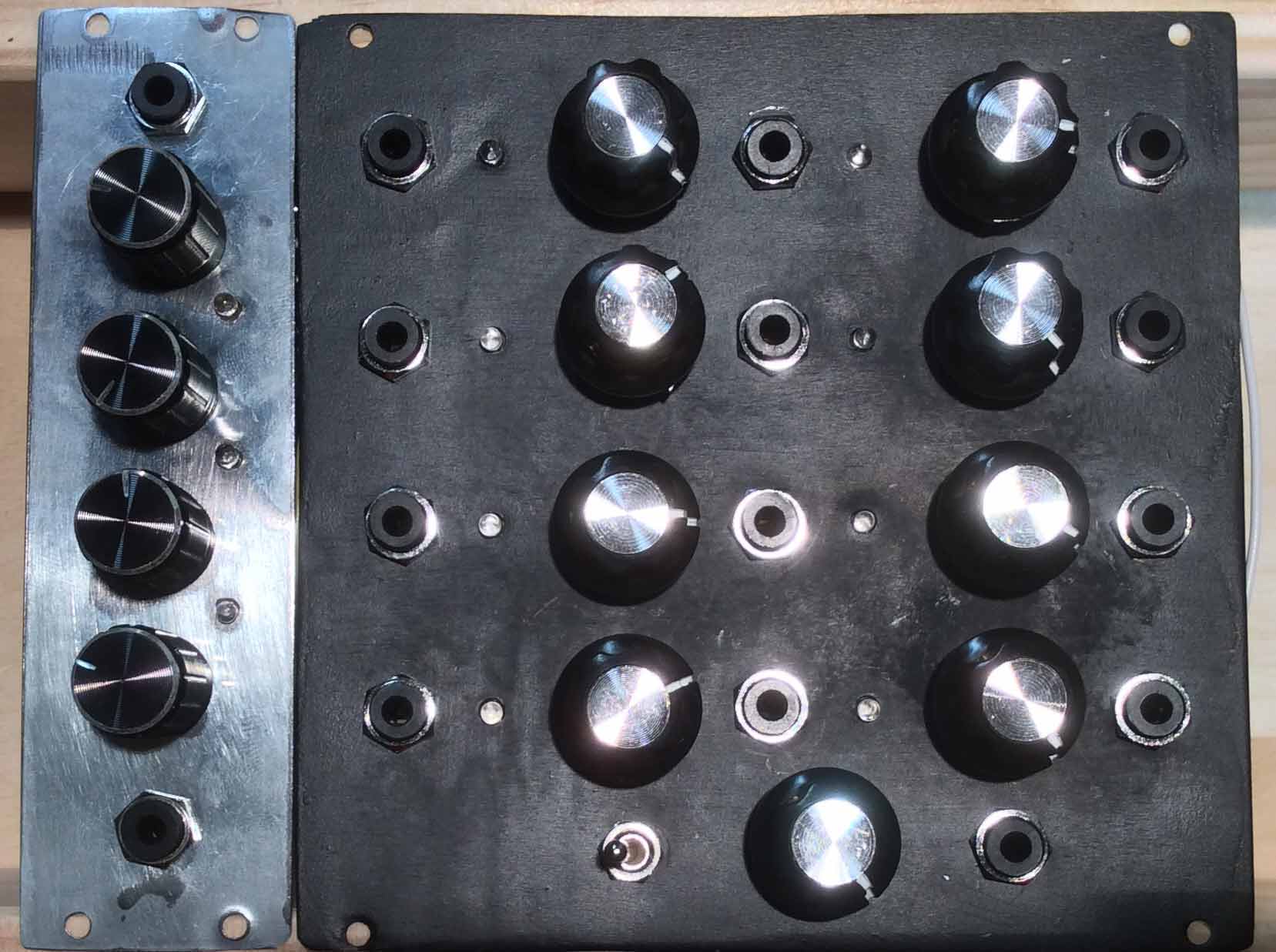
I’m pleased how this project turned out. Making interesting melodies with the limitations of a CD4017 chip is surprisingly fun. I’m now seeing the need for an oscillator with a wider frequency bandwidth. The Triple oscillator is very limited in terms of usable chords to make a melody with. This is a really straightforward device to build. If you can solder and follow a schematic, you can build a Baby 8.